Schematic-ready two-channel Rev-A architecture with protected analog inputs, SPI conversion, framed USB transport, and a Python host workflow.
Schematic-ready design
Analytical calculation
Automated test
Problem statement
Design a buildable first-revision acquisition board that exposes the real interfaces among analog conditioning, conversion, firmware buffering, USB transport, layout, and verification without overstating unbuilt hardware.
A mixed-signal design package connecting electrical requirements and PCB constraints to portable embedded logic, host-side capture, and an explicit hardware bring-up plan.
20 kS/s/ch
Sampling target
Two channels; not yet measured on target hardware
12 bit
Nominal conversion
0.806 mV ideal LSB at a 3.3 V reference
10.61 kHz
Input RC pole
First-order anti-alias aid above the 5 kHz useful band
250 kHz
PWM carrier
Filtered for slow analog stimulus, not precision generation
Project scope
Two protected 0-3.0 V inputs and a 20 kS/s-per-channel target
250 kHz PWM with a two-pole RC output for slow stimulus and loopback testing
Schematic-ready connections and layout plan; no KiCad PCB, fabrication, or bench measurements
System or processing architecture
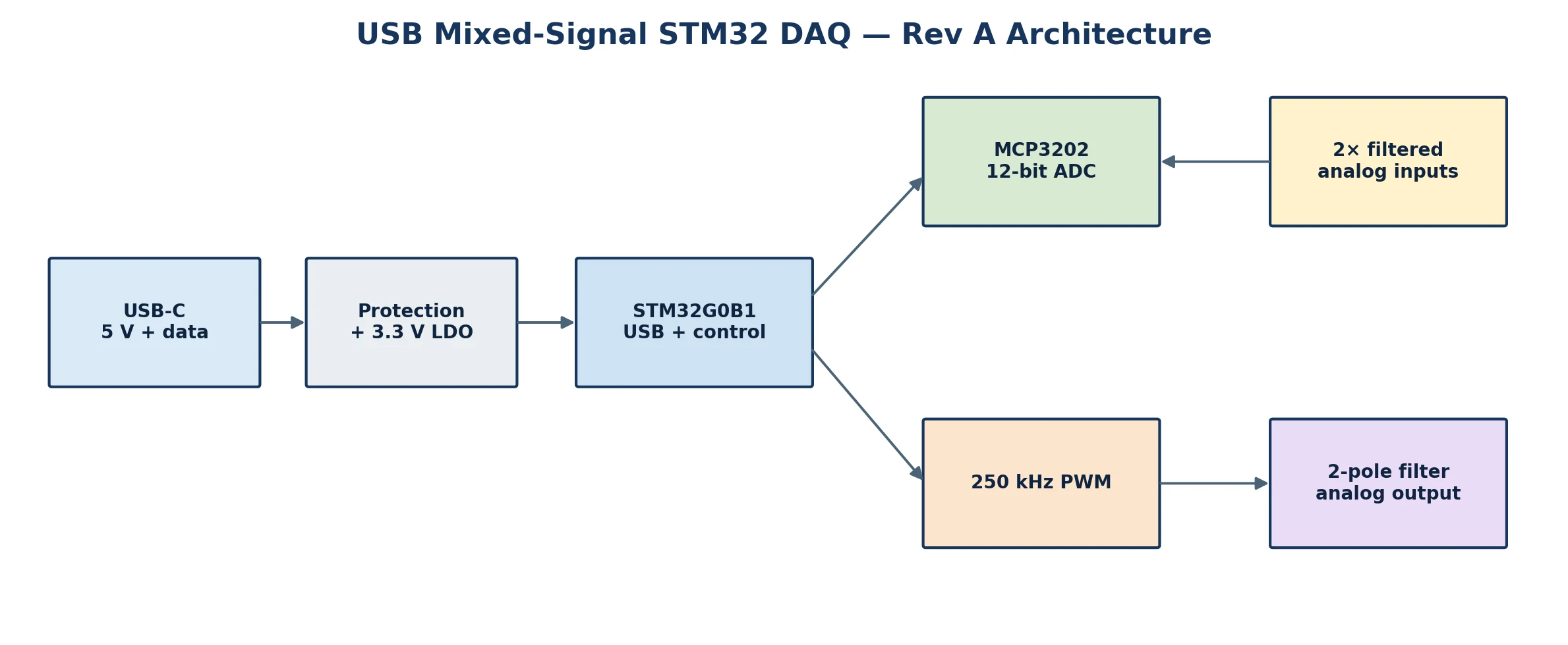
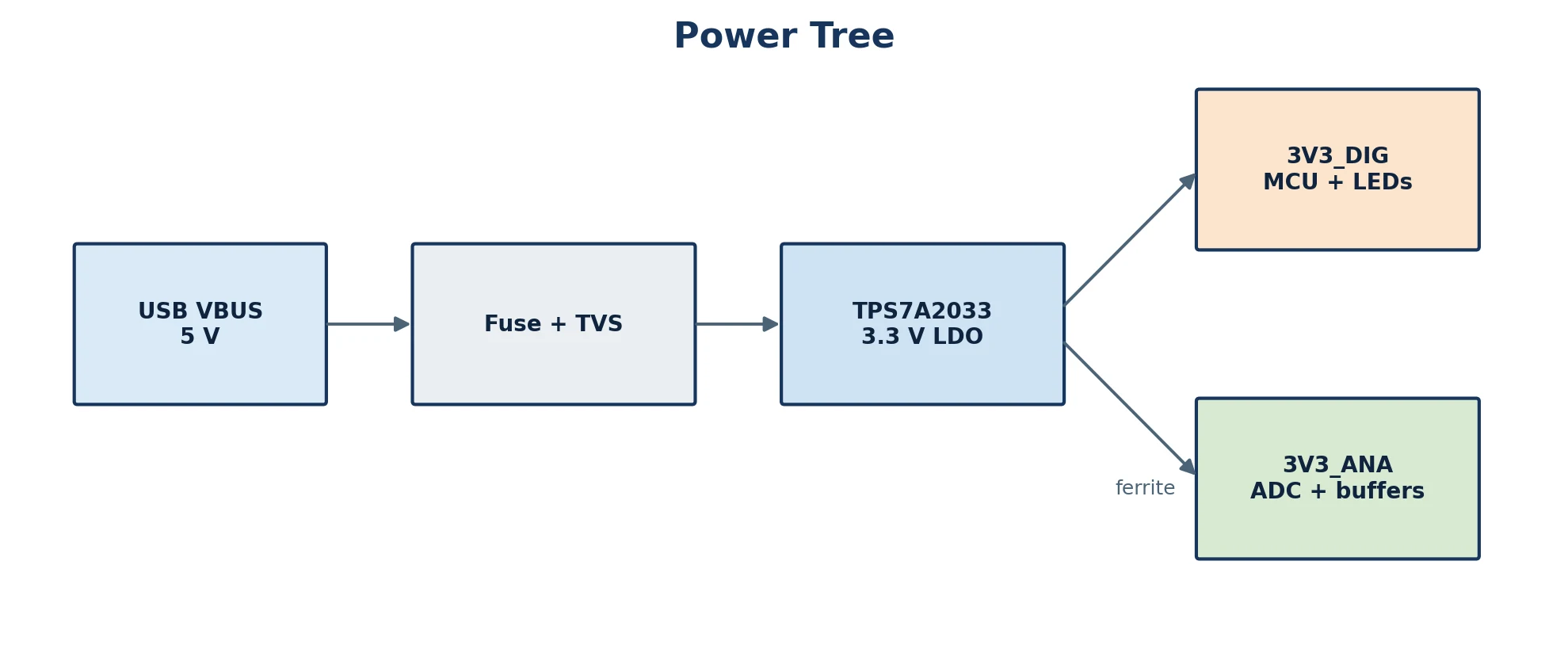
USB-C supplies 5 V and CDC transport. A protected LDO creates digital 3.3 V and a ferrite-fed analog zone over one continuous ground plane. Buffered RC-filtered inputs feed the external ADC; timer-driven firmware fills ping-pong buffers and emits sequence- and CRC-protected frames.
My engineering contributions
Converted acquisition goals into measurable electrical, timing, interface, and bring-up requirements.
Selected the MCU, ADC, op amp, regulator, protection approach, and assembly-friendly packages through a documented trade study.
Defined schematic-ready connections, pin assignments, floorplan, return-path rules, BOM, and Rev-A risk controls.
Implemented portable buffering, framing, CRC, PWM math, and a Python parser/simulated capture workflow.
Important design decisions
Selected a 12-bit SOIC ADC over a higher-resolution delta-sigma device to reduce Rev-A clocking, front-end, and assembly risk.
Used one continuous ground plane with placement-based analog/digital partitioning to preserve return-current paths.
Kept USB transfer outside the sampling callback and added sequence, status, and CRC fields so transport failures are observable.
Engineering methods
RC cutoff, quantization, power, and ideal PWM-ripple calculations
Mixed-signal placement and return-path planning
Ping-pong acquisition buffering and CRC-16-CCITT framing
Native C unit tests and host parser simulation
Staged power, USB, ADC, output, loopback, and sustained-stream bring-up plan
Selected evidence
Readable results, with context
Figure 1Rev-A functional architecture linking USB power/data, conversion, acquisition control, and filtered output.
Figure 2Power and placement domains share one continuous ground plane; the ferrite separates supply noise, not ground nets.
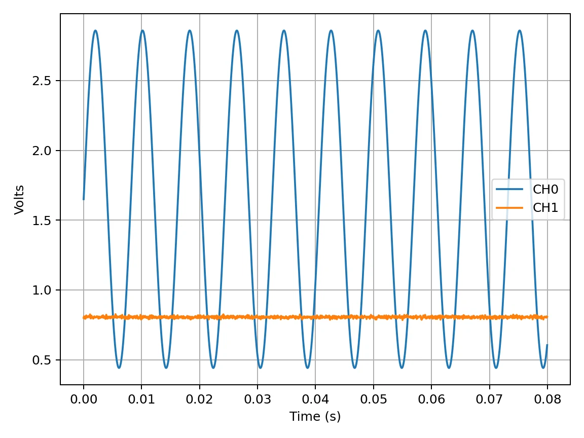
Figure 3Host-side simulated capture verifies parsing, engineering-unit conversion, CSV export, and plotting—not analog hardware performance.
Verification and testing
The calculation script produces filter, quantization, thermal, data-rate, and supply-current results.